
Silicon Valley, the epitome of technological innovation, serves as the birthplace of countless advancements that have shaped our digital landscape. Within this bustling hub of creativity and progress, one crucial yet often overlooked component plays a pivotal role in ensuring the efficiency of semiconductor devices - the Probe Card. We delve into the world of Probe Card Design in California, where precision meets technology.
What is a Probe Card?
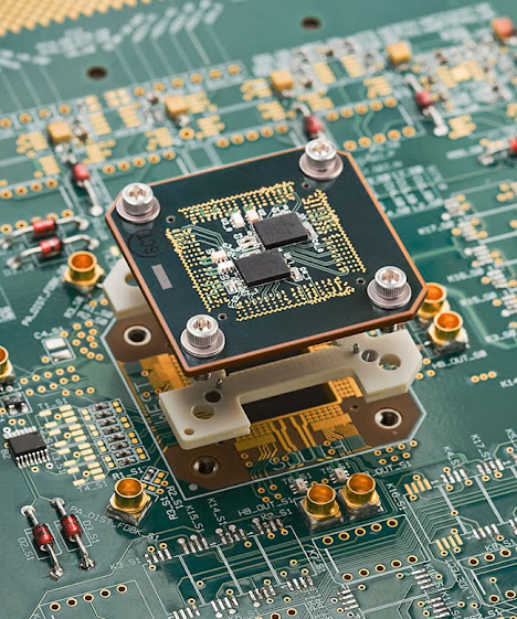
At its core,
a Probe Card is a specialized electronic test tool used to perform wafer
testing during the semiconductor manufacturing process. It acts as the
intermediary between the testing equipment and the semiconductor wafer,
ensuring that each chip meets the required standards before being integrated
into the final product. The significance of this seemingly small device cannot
be overstated, as it directly impacts the quality and reliability of the end
product.
Why is Silicon Valley The Hub of Probe Card Design?
- Technological Innovation
Silicon
Valley is synonymous with technological innovation, and the field of Probe Card
Design is no exception. The region hosts a concentration of top-tier technology
companies and research institutions that constantly push the boundaries of what
is possible. This environment fosters collaboration and competition, driving
the continuous improvement of Probe Card technology.
- Access to Skilled Talent
The
abundance of skilled professionals in Silicon Valley contributes significantly
to the region's dominance in Probe Card Design. Engineers and designers with
expertise in semiconductor testing and precision engineering are drawn to the
area, creating a talent pool that is crucial for developing cutting-edge Probe
Card solutions.
The Anatomy of Probe Card Design:
- Microfabrication Techniques
The heart of
any Probe Card lies in its microfabricated components. Precision is key in this
stage, as the tiny probes must be designed to make accurate contact with the
semiconductor wafer. Microfabrication techniques involve intricate processes
such as photolithography and etching, ensuring that each probe is crafted with
the utmost precision.
- Material Selection
The choice
of materials for Probe Card construction is critical to its performance.
Factors such as conductivity, durability, and thermal stability are carefully
considered. In California, where environmental consciousness is high, there is
also a focus on sustainable and eco-friendly materials, aligning with the
region's commitment to green technology.
- Advanced Calibration
Calibrating
a Probe Card is a meticulous process that involves adjusting its parameters to
ensure accurate and reliable testing results. Advanced calibration techniques,
often developed in the R&D labs of Silicon Valley, contribute to the
precision and efficiency of Probe Cards, making them an indispensable tool in
semiconductor manufacturing.
Challenges and Innovations in Probe Card Design:
- Shrinking Semiconductor Sizes
As
semiconductor technology advances, the size of individual components continues
to shrink. This poses a significant challenge for Probe Card and Design, as the
probes must be small enough to make contact with these minuscule structures
without compromising accuracy. Innovations in nanotechnology and
microfabrication are essential to address this ongoing challenge.
- Increasing Testing Complexity
The demand
for more powerful and feature-rich semiconductor devices has led to an increase
in testing complexity. Probe Cards must now accommodate a wide range of testing
parameters and ensure reliable results across diverse semiconductor designs.
This complexity drives continuous innovation in Probe Card Design to keep pace
with the evolving semiconductor landscape.
The Future of Probe Card Design in California:
- Integration of Artificial Intelligence
As
artificial intelligence (AI) continues to permeate various industries, Probe
Card Design is no exception. AI algorithms can be employed to optimize testing
processes, analyze vast amounts of data, and enhance the overall efficiency of
semiconductor testing. The intersection of AI and Probe Card Design in
California is an exciting frontier that holds the potential to revolutionize
the industry.
- Collaboration for Advancements
The
collaborative spirit of Silicon Valley is a driving force for future
advancements in Probe Card and Design. Companies, research institutions, and
startups come together to share insights, pool resources, and collectively
tackle the challenges that lie ahead. This collaborative ecosystem ensures that
California remains at the forefront of Probe Card innovation.